|

|


Electromagnetic wave (EM) pollution such as signals hanphone, hotspot, reuter, television, and so on which are generated from electronic equipment can disrupt human activities and instrumentation systems on the earth's surface.
To help avoid the pollution effects caused by electronic equipment, Yuda Bakti Zainal, Doctor of FMIPA UI from the Materials Science Study Program developed a composite system EM wave absorbing material that combines dielectric and magnetic materials. The material synthesis method used is mechanical alloying or mechanical blending.
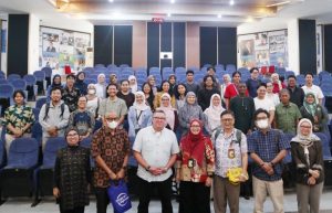
"Currently, the use of electronic devices cannot be avoided by society, and tends to increase. The increase in the number of electronic devices used can cause electromagnetic wave (EM) pollution around us," said Dr. Yuda opening his dissertation presentation at the Open Session of Doctoral Promotion, at FMIPA UI, Depok, Thursday (4/7).
In his dissertation entitled In the Development of Dielectric Materials Through Nano Composite Systems [BaTi entitled(1-x)ZnxO3](1-y)-[CoFe2O4]y (x = 0; 1/3; 1/2; 2/3; 1; and y = 0.2; 0.5; 0.8) for Electromagnetic Wave Absorber Applications, Dr. Yuda explained that electromagnetic interference problems or electromagnetic wave interference (EMI) has become a widespread problem and is beginning to be considered collectively by researchers, particularly regarding the use of electronic equipment that uses EM waves in the 8-12 GHz frequency range (X-band). EMI itself is an uncontrolled and unwanted radiation signal resulting from interference with radiation signals emitted from electronic equipment.
The Electrical Engineering lecturer at the Faculty of Engineering, Jenderal Achmad Yani University emphasized that an effective method is needed for protection from the impact of EMI.
"This protection can be achieved in two ways; the first is by using a shielding method, and the second is by using an EM wave absorber using EM materials that can interact in a complex reciprocal manner between the EM field and the electron material system," he added to the testing team.
Unfortunately, shielding methods are difficult to eliminate or attenuate EMI radiation. They can even create new frequency interference due to incoming EM waves interacting with reflected EM waves, which can interfere with other electronic devices. Therefore, the best method is the second method, which uses EM wave-absorbing materials that can transfer the energy of the interfering EM waves into other forms, such as heat energy.
The EM wave absorbing material can be made from dielectric and/or magnetic materials that can absorb EM waves, thereby weakening EMI radiation.
Through his research, Yuda Bakti Zainal earned a Doctorate with a very satisfactory predicate under the guidance of Prof. Dr. Azwar Manaf, M.Met. (Professor of Materials Science, FMIPA UI) as promoter, and Dr. Dedi, M.T. (Expert Condensed Matter Physics National Research and Innovation Agency) as Co-Promoter.
During his studies and research, Dr. Yuda received guidance and support facilities from the Postgraduate Program in Materials Science, FMIPA UI, and the Center for Advanced Materials Research, National Research and Innovation Agency (BRIN) Bandung.
He hopes that the results of his research can be developed by compositing the dielectric material BaTiO3 with graphene/polyurethane to expand bandwidth from RL and is recommended as an anti-radar detection paint material or a protective coating from EMI radiation.
News source : https://sci.ui.ac.id/